
ESE101: Microcontroller Peripherals, GPIOs, and Blinking Lights: Part 3
We ended Part 2 last week with this picture which shows the memory mapped GPIO Port 1 and Port 2 control registers in the MSP430’s memory map at locations 0x0200-0x021F:

This week we’ll connect the abstract drawings and ideas to reality by walking through how the code actually turns on an LED.
To find out the specifics of how the MSP430’s GPIOs are configured we need to go to the MSP430’s User Guide and go to chapter 12, “Digital I/O Module.” There you’ll see that the MSP430 has several control registers used to control the GPIOs. I won’t quote the document here, instead here’s a summary:
- The three main control registers for GPIO port P1 are P1DIR, P1OUT, and P1IN.
- Each of those three registers is 8-bits wide.
- Each bit in each register corresponds to one GPIO pin. Bit 0 corresponds to port P1 pin 0, bit 1 corresponds to port P1 pin 1, and so on up to bit 7 corresponds to port P1 pin 7.
- P1DIR: each bit in P1DIR sets the direction of the corresponding GPIO pin: 0 = input, 1 = output.
- P1OUT: if the GPIO pin is configured as an output in P1DIR, the corresponding bit in P1OUT sets the voltage level on the pin: 0 = output is low, 1 = output is high.
- P1IN: if the GPIO pin is configured as an input in P1DIR, the corresponding bit in P1IN is the value on the pin: 0 = input is low, 1 = input is high.
Let me make it more concrete: to configure GPIO P1 pin 0 as an output and set the output pin to high you would:
- Set P1DIR bit 0 to 1:
- The C code for doing this is: P1DIR |= 0x01;
- This configures P1 pin 0 as an output.
- Set P1OUT bit 0 to 1:
- The C code for doing this is: P1OUT |= 0x01;
- This sets P1 pin 0 as a high voltage output.
Note: The C operator “|=” is a “bitwise or assignment” operation. |= takes whatever value is originally in P1DIR or P1OUT, does a bitwise or with 0x01, which sets bit 0 in P1DIR or P1OUT to 1. We’ll cover C later, so if this seems confusing it’s okay to take my word for it for now. Or if you can't wait please check out Andrei's intro to C in his Embedded Wednesdays posts.
Let’s make it even more concrete by looking at how the blinky example turns on and off its LED.
Plug in your MSP430 LaunchPad board and start Code Composer Studio with the blinky example from a few weeks ago. If you modified or lost the blinky example, see the original post for how to create a new blinky example.
Select Run->Debug and CCS will download the code to the MSP430 chip over USB, and start a debugger at the blinky code’s main function. Now click the Registers tab in the upper right-hand window of CCS to show the registers. Scroll down in the Registers view and click on the arrow to open the “Port_1_2” item. It should look something like this:

“Port_1_2” is the GPIO P1 and P2 peripheral configuration register space. You should recognize the P1IN, P1OUT, and P1DIR register names.
Now let’s see what MSP430 instructions are actually running on the microcontroller. Select View->Disassembly to bring up the Disassembly view like this:

The Disassembly view shows you the assembly instructions that are actually running on the microcontroller. CCS shows the line that’s about to execute highlighted in green in both the C source view and the Disassembly view. The screenshot above shows the microcontroller at the start of execution, before it has started running the blinky main code.
The Disassembly view helpfully shows us the assembly code right below the corresponding C instruction for that instruction, like this:

You can see that the C code to set the GPIO direction to output is:
P1DIR |= 0x01;
And it's turned into the assembly code:
BIS.B #1, &PORT_A_P1DIR
That C code is setting bit 0 in the P1DIR register to 1 using the “|=” bitwise or assignment operator. The P1DIR variable in the C code is cleverly defined by the TI-provided support code to live at address location where the P1DIR configuration registers lives.
That assembly instruction BIS is the bit set instruction, which sets bit 0 in the PORT_A_P1DIR location. You know what P1DIR means, but what is “PORT_A”? PORT_A is how the MSP430 refers to the combination of Ports 1 and 2. It’s a little confusing: Port 1 is the name of a GPIO peripheral with 8 pins. Port 2 is the name of another GPIO peripheral with 8 pins. PORT_A is the name used to refer to both Port 1 and Port 2 at the same time. As long as you understand that PORT_A_P1DIR refers to the Port 1 P1DIR configuration register you’re all set.
Let’s go look at the memory assigned to the GPIO Port 1 configuration registers. Remember the MSP430 datasheet says that GPIO Port 1 configuration registers start at address 0x0200; Select View->Memory Browser, and type in “0x0200” where it says “Enter location here” in the Memory Browser window that pops up. You should see this:

Then change the drop-down menu selection from “16-Bit Hex - TI Style” to “8-Bit Hex - TI Style” so we can see each 8-bit register on its own. You should see something like this:
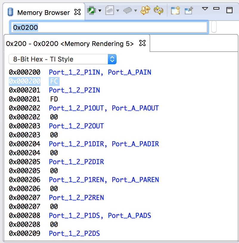
The Memory Browser is showing you that address 0x0200 corresponds to Port_1_2_P1IN and its value is 0xFC. Port_1_2_P1IN is the P1IN control register of the GPIO Port 1 and 2 peripheral address space. (Remember that Ports 1 and 2 share the same peripheral address space.) P2IN is at address 0x0201 with current value 0xFD, P1OUT is at 0x0202 with current value 0x00, and so on - this agrees with what we’ve learned about GPIO configuration from the TI documentation, which is good!
The Registers window and the Memory Browser window are showing you two different views of the same data: the Registers window’s data is populated by the debugger reading the memory locations for the peripheral, which is the same way the Memory Browser window gets its data. Normally while debugging I’ll use just the Registers view to check how the peripheral is configured because the formatting is better. I’m showing you both the Registers and Memory Browser windows to reinforce the fact that peripheral configuration registers are accessed as memory addresses.
Now let’s run a couple lines of code and watch the GPIO configuration change.
Select “Run->Step Into” two times and the green highlight bar should be over the P1DIR |= 0x01; line in the C source window and the BIS #1, &Port_A_PADIR line in the Disassembly window.
The Registers window should show P1DIR = 0, and so should the Memory Browser window (look for address 0x0204 for P1DIR).
Select Run->Step Into once and watch how the P1DIR value changes in the Registers and Memory Browser windows; the Registers window will highlight changes in yellow, and the Memory Browser in red:

P1DIR changes to 1 in both windows: this means that P1DIR bit 0 is now set to 1. P1 pin 0 is now configured as an output.
The program is now waiting at the C code which should actually flip bit 0 in the P1OUT register:
P1OUT ^= 0x01;
Note: “^=” applies the “bitwise XOR assignment operation” to P1OUT. XOR’ing P1OUT with 0x01 toggles bit 0 in P1OUT each time the XOR operation runs.
And the corresponding assembly instruction is the XOR byte instruction:
XOR.B #1,&Port_A_PAOUT
Select Run->Step Into one more time to run that code. The LED should turn on and P1OUT should now be ‘1’ in the Registers and Memory Browser windows:

Success! P1OUT has changed to 1, meaning that its bit 0 is now 1. When this bit is set to 1 the MSP430 puts a high voltage output on GPIO P1 bit 0, which is connected to the LED (marked as P1.0 on the circuit board), and this high voltage turns the LED on.
To further drive home the point, let’s turn the light on and off by manually changing the memory. Click on the value of Port_1_2_P1OUT in the Memory Browser window, which should be the red “01” currently, and change the “01” to “00”, then hit enter. You’ve just manually changed the P1OUT bit 0 value from 1 to 0, which should turn off the light. Now change that “00” back to a “01” to change bit 0 back to 1 and I’ll bet you can guess what should happen - the light should turn back on.
You can do the same thing by changing the P1OUT values in the Registers window. Remember that both the Memory Browser and Register windows use the underlying memory addresses to interact with the peripheral control registers; they’re two views of the same thing.
You should be amazed at what you just did! With a little bit of typing and mouse clicking you’ve altered the flow of electrons on a circuit board and caused electricity to flow through an LED and turned a light on.
Seriously, I hope you stop for a second and are at least a little pleased. Please allow me to wax poetic for a moment:
THIS IS AMAZING! YOU HAVE CONTROLLED ELECTRICITY! YOU HAVE BENT NATURE TO YOUR WILL! YOU HAVE CHANGED THE PHYSICAL WORLD BY TYPING!!!
I’ve been doing this stuff professionally since 2002 and I still think it’s magical when it works. Of course when it doesn’t work, usually due to my own faulty code, it’s far less than magical, but the success is worth the effort!
If you think this is as cool as I do, then perhaps embedded software is the right field for you.
(And if you've ever considered working for a cool robotics company, you should check out iRobot's careers site and email me your resume at csvec at iRobot's domain. We hire embedded and non-embedded engineers, including test and iOS software engineers. I'm always happy to hear from interested readers even if it's not a great match at the moment.)
Now you know how peripherals are documented and configured, how to control GPIOs, and how to turn an LED on!
I threw a lot of words and concepts at you in these three posts. Take a moment to look at the high-level diagram again:

If you understand that picture, then you understand the basics of GPIO peripherals. If something isn’t clear, then please say something in the comments and I’ll be more than happy to try to explain it better. Thanks for reading!
This post is part of a series. Check out the complete Embedded Software Engineering 101 series here.